Zedboard_Custom_IP

ZedBoard turn on Light by launching SDK and Custom IP


1、Create Project

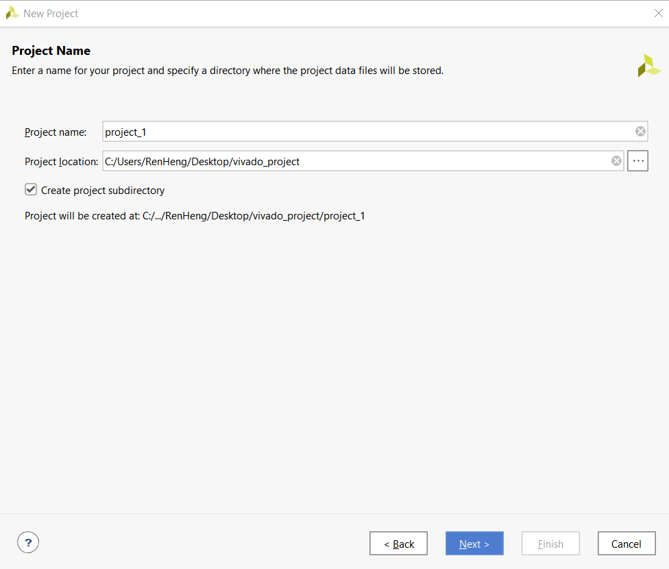
Project Name -> RTL Project -> Next -> Choose “Boards / ZedBoard Zynq Evaluation and Development Kit” -> Finish
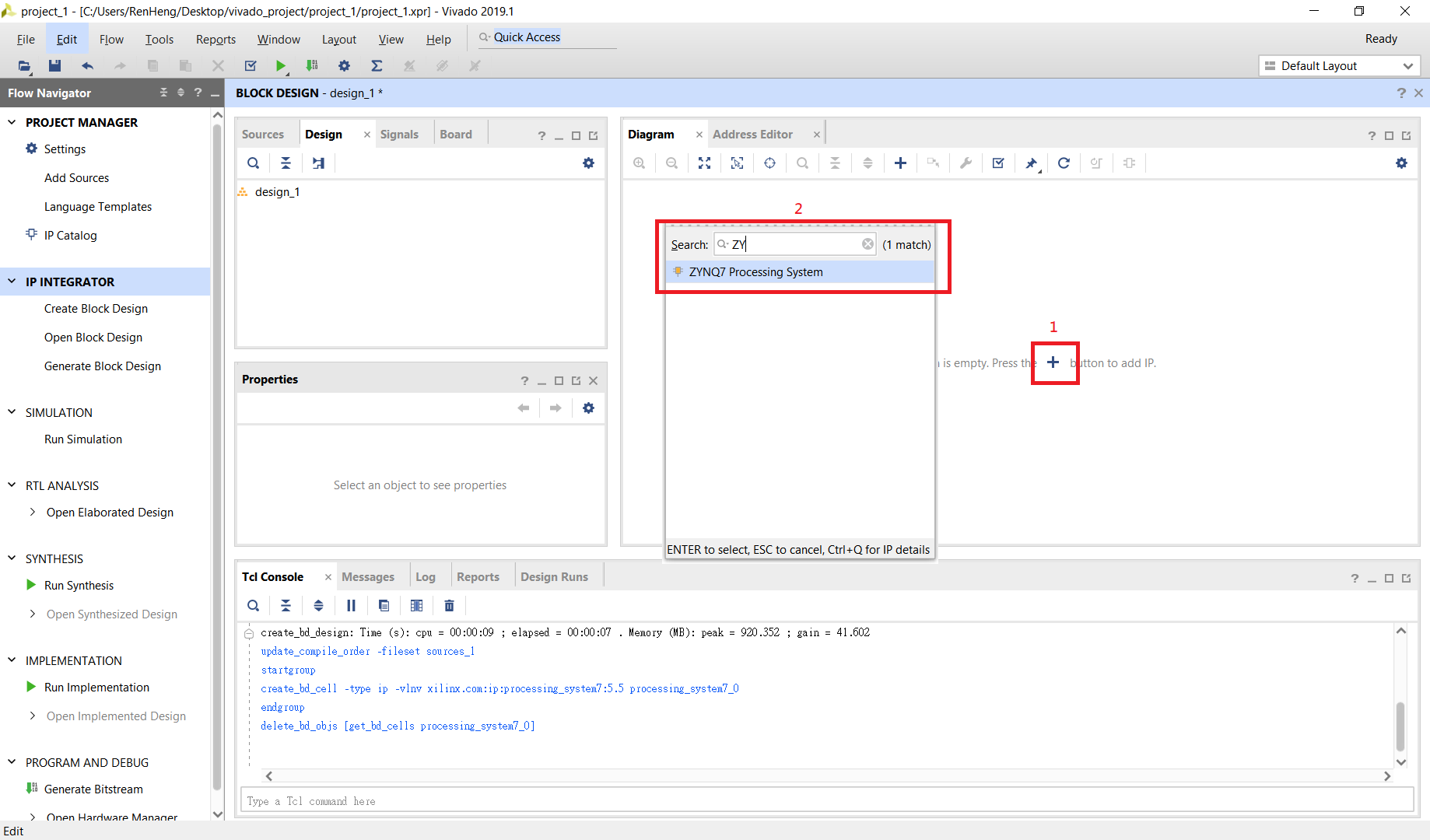

2、Custom IP

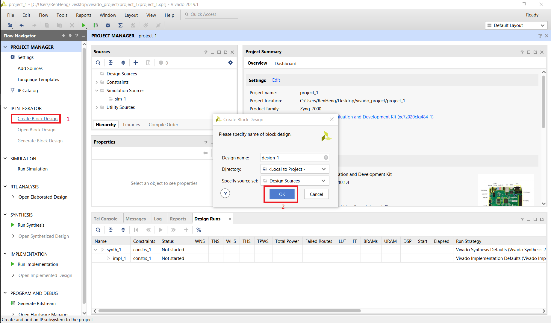
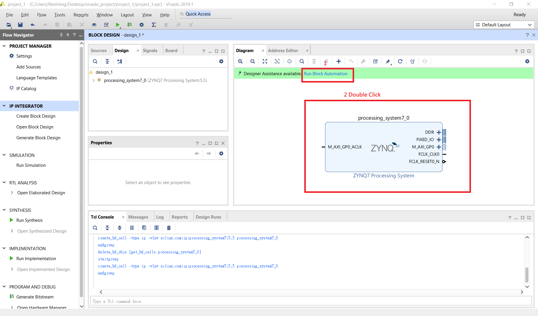
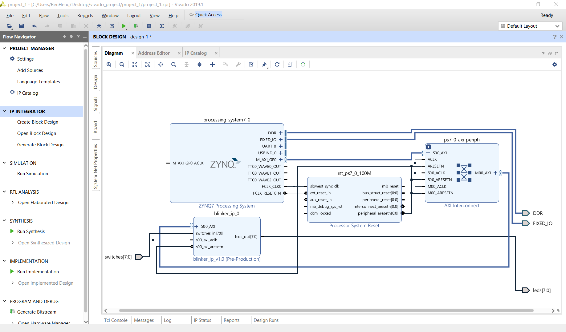
Create Block Design -> add IP -> search “ZYNQ7 Processing System -> Run Block Automation -> OK

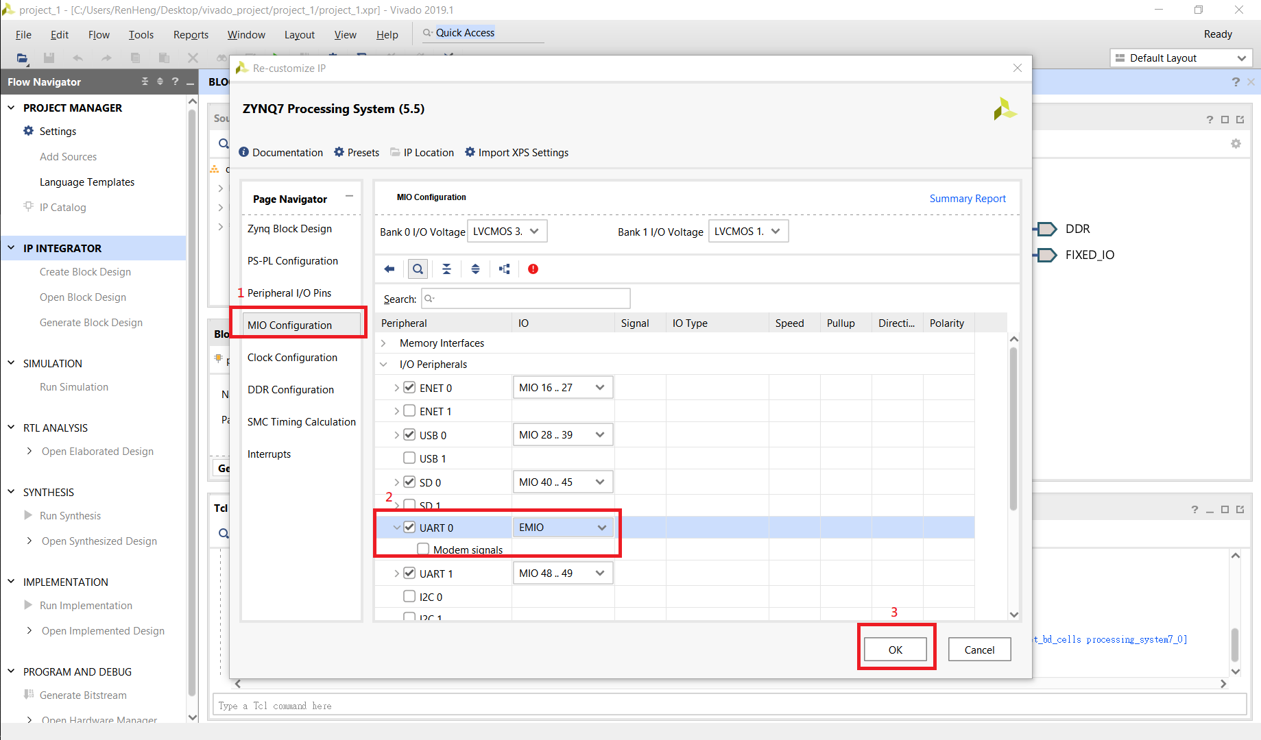
Double Click ZYNQ -> Add UART 0 port

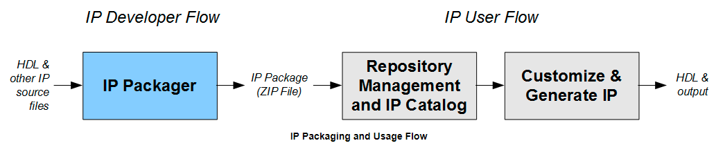
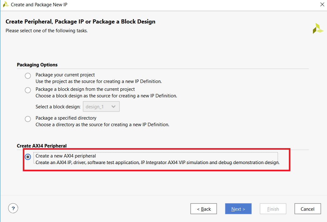
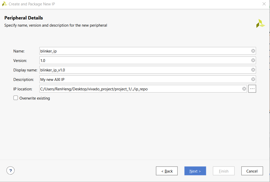
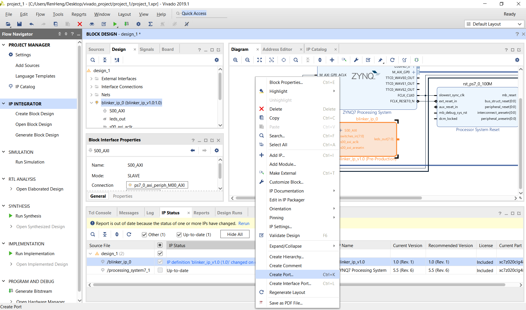
Create and package New IP

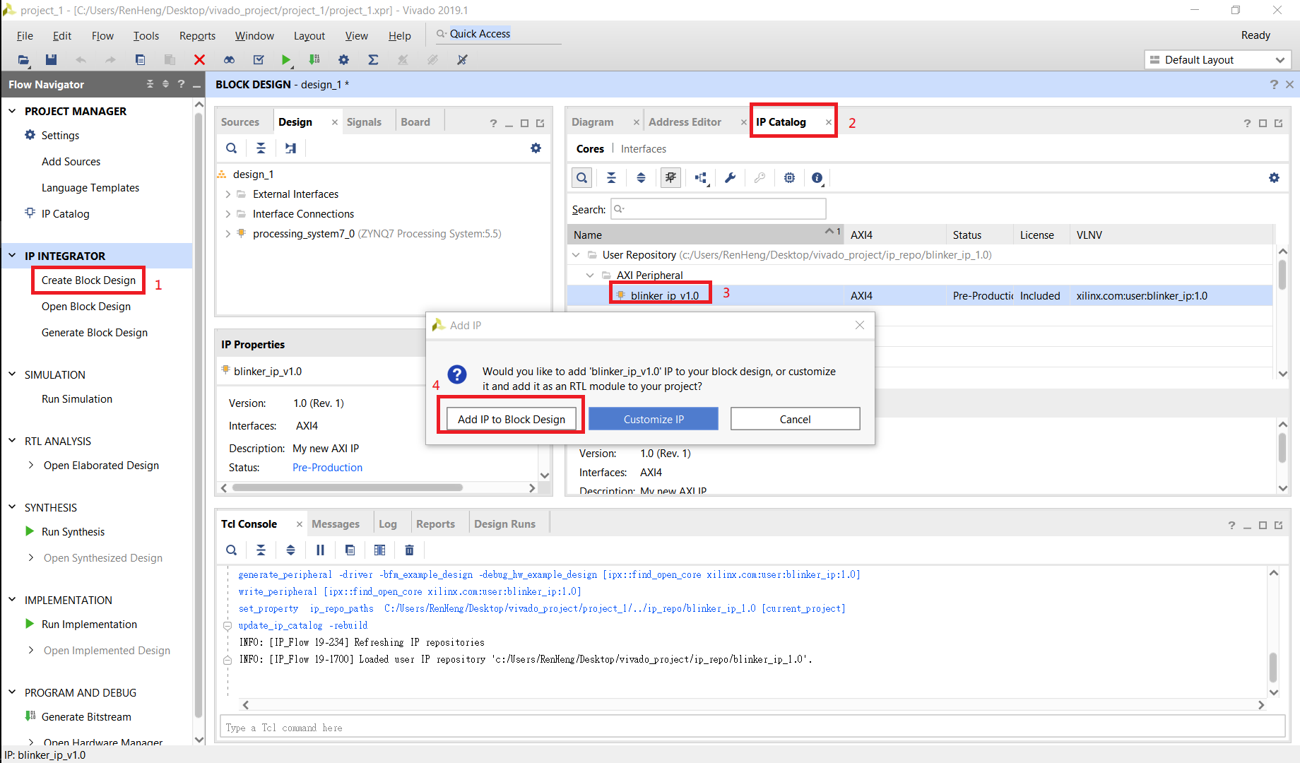
Edit in IP Package : Right click “Blinker_ip_0” and choose Edit in IP Package -> ok
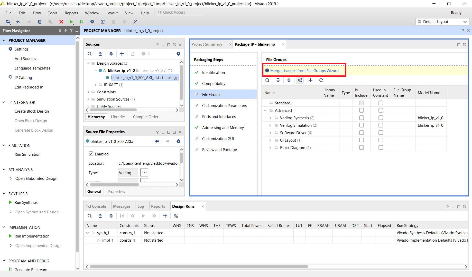
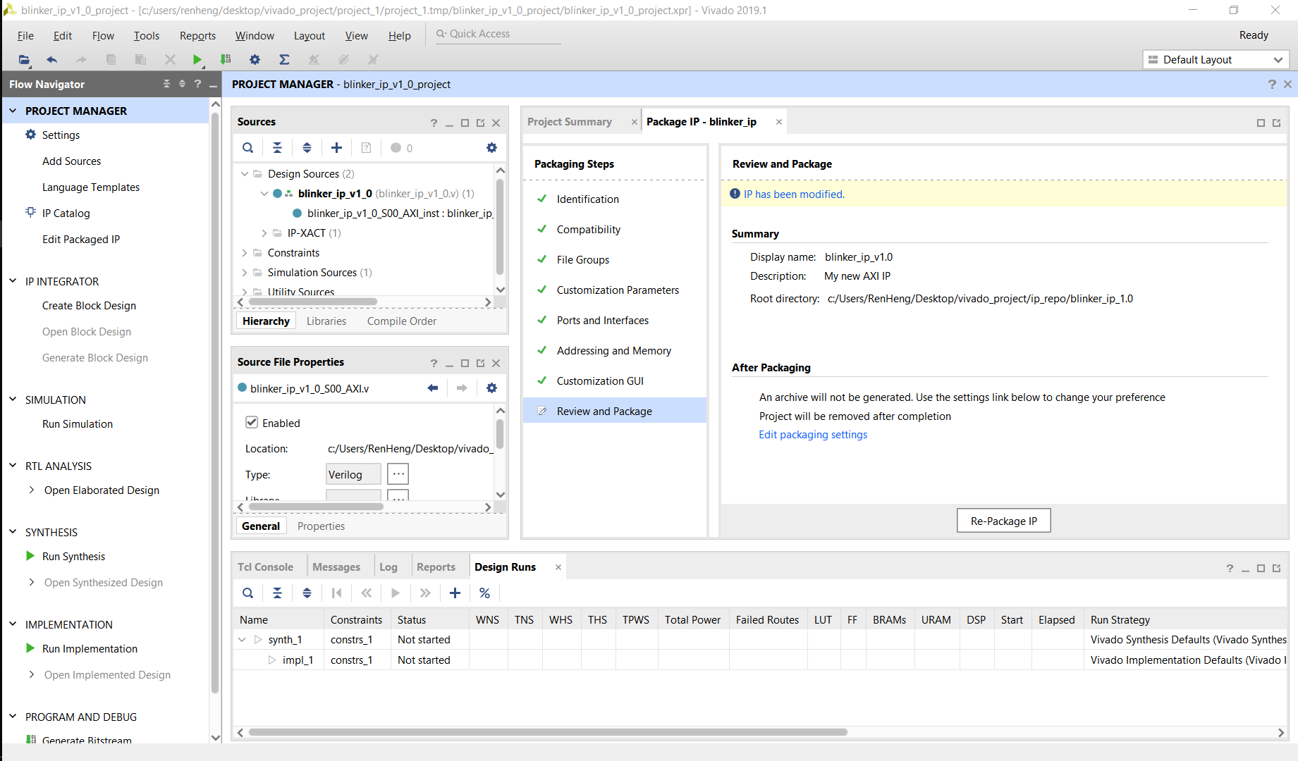
1
2
3
4
5
6
7
8
9
10
11
12
13
14
15
16
17
18
19
20
21
22
23
24
25
26
27
28
29
30
31
32
33
34
35
36
37
38
39
40
41
42
43
44
45
46
47
48
49
50
51
52
53
54
55
56
57
58
59
60
61
62
63
64
65
66
67
68
69
70
71
72
73
74
75
76
77
78
79
80
81
`timescale 1 ns / 1 ps

module blinker_ip_v1_0 #
(
// Users to add parameters here

// User parameters ends
// Do not modify the parameters beyond this line


// Parameters of Axi Slave Bus Interface S00_AXI
parameter integer C_S00_AXI_DATA_WIDTH = 32,
parameter integer C_S00_AXI_ADDR_WIDTH = 4
)
(
// Users to add ports here
input wire [7:0] switches_in,
output wire [7:0] leds_out,
// User ports ends
// Do not modify the ports beyond this line


// Ports of Axi Slave Bus Interface S00_AXI
input wire s00_axi_aclk,
input wire s00_axi_aresetn,
input wire [C_S00_AXI_ADDR_WIDTH-1 : 0] s00_axi_awaddr,
input wire [2 : 0] s00_axi_awprot,
input wire s00_axi_awvalid,
output wire s00_axi_awready,
input wire [C_S00_AXI_DATA_WIDTH-1 : 0] s00_axi_wdata,
input wire [(C_S00_AXI_DATA_WIDTH/8)-1 : 0] s00_axi_wstrb,
input wire s00_axi_wvalid,
output wire s00_axi_wready,
output wire [1 : 0] s00_axi_bresp,
output wire s00_axi_bvalid,
input wire s00_axi_bready,
input wire [C_S00_AXI_ADDR_WIDTH-1 : 0] s00_axi_araddr,
input wire [2 : 0] s00_axi_arprot,
input wire s00_axi_arvalid,
output wire s00_axi_arready,
output wire [C_S00_AXI_DATA_WIDTH-1 : 0] s00_axi_rdata,
output wire [1 : 0] s00_axi_rresp,
output wire s00_axi_rvalid,
input wire s00_axi_rready
);
// Instantiation of Axi Bus Interface S00_AXI
blinker_ip_v1_0_S00_AXI # (
.C_S_AXI_DATA_WIDTH(C_S00_AXI_DATA_WIDTH),
.C_S_AXI_ADDR_WIDTH(C_S00_AXI_ADDR_WIDTH)
) blinker_ip_v1_0_S00_AXI_inst (
.S_AXI_ACLK(s00_axi_aclk),
.S_AXI_ARESETN(s00_axi_aresetn),
.S_AXI_AWADDR(s00_axi_awaddr),
.S_AXI_AWPROT(s00_axi_awprot),
.S_AXI_AWVALID(s00_axi_awvalid),
.S_AXI_AWREADY(s00_axi_awready),
.S_AXI_WDATA(s00_axi_wdata),
.S_AXI_WSTRB(s00_axi_wstrb),
.S_AXI_WVALID(s00_axi_wvalid),
.S_AXI_WREADY(s00_axi_wready),
.S_AXI_BRESP(s00_axi_bresp),
.S_AXI_BVALID(s00_axi_bvalid),
.S_AXI_BREADY(s00_axi_bready),
.S_AXI_ARADDR(s00_axi_araddr),
.S_AXI_ARPROT(s00_axi_arprot),
.S_AXI_ARVALID(s00_axi_arvalid),
.S_AXI_ARREADY(s00_axi_arready),
.S_AXI_RDATA(s00_axi_rdata),
.S_AXI_RRESP(s00_axi_rresp),
.S_AXI_RVALID(s00_axi_rvalid),
.S_AXI_RREADY(s00_axi_rready),

.switches_in(switches_in),
.leds_out(leds_out)
);

// Add user logic here

// User logic ends

endmodule
1
2
3
4
5
6
7
8
9
10
11
12
13
14
15
16
17
18
19
20
21
22
23
24
25
26
27
28
29
30
31
32
33
34
35
36
37
38
39
40
41
42
43
44
45
46
47
48
49
50
51
52
53
54
55
56
57
58
59
60
61
62
63
64
65
66
67
68
69
70
71
72
73
74
75
76
77
78
79
80
81
82
83
84
85
86
87
88
89
90
91
92
93
94
95
96
97
98
99
100
101
102
103
104
105
106
107
108
109
110
111
112
113
114
115
116
117
118
119
120
121
122
123
124
125
126
127
128
129
130
131
132
133
134
135
136
137
138
139
140
141
142
143
144
145
146
147
148
149
150
151
152
153
154
155
156
157
158
159
160
161
162
163
164
165
166
167
168
169
170
171
172
173
174
175
176
177
178
179
180
181
182
183
184
185
186
187
188
189
190
191
192
193
194
195
196
197
198
199
200
201
202
203
204
205
206
207
208
209
210
211
212
213
214
215
216
217
218
219
220
221
222
223
224
225
226
227
228
229
230
231
232
233
234
235
236
237
238
239
240
241
242
243
244
245
246
247
248
249
250
251
252
253
254
255
256
257
258
259
260
261
262
263
264
265
266
267
268
269
270
271
272
273
274
275
276
277
278
279
280
281
282
283
284
285
286
287
288
289
290
291
292
293
294
295
296
297
298
299
300
301
302
303
304
305
306
307
308
309
310
311
312
313
314
315
316
317
318
319
320
321
322
323
324
325
326
327
328
329
330
331
332
333
334
335
336
337
338
339
340
341
342
343
344
345
346
347
348
349
350
351
352
353
354
355
356
357
358
359
360
361
362
363
364
365
366
367
368
369
370
371
372
373
374
375
376
377
378
379
380
381
382
383
384
385
386
387
388
389
390
391
392
393
394
395
396
397
398
399
400
401
402
403
404
405
406
`timescale 1 ns / 1 ps

module blinker_ip_v1_0_S00_AXI #
(
// Users to add parameters here

// User parameters ends
// Do not modify the parameters beyond this line

// Width of S_AXI data bus
parameter integer C_S_AXI_DATA_WIDTH = 32,
// Width of S_AXI address bus
parameter integer C_S_AXI_ADDR_WIDTH = 4
)
(
// Users to add ports here
input wire [7:0] switches_in,
output wire [7:0] leds_out,
// User ports ends
// Do not modify the ports beyond this line

// Global Clock Signal
input wire S_AXI_ACLK,
// Global Reset Signal. This Signal is Active LOW
input wire S_AXI_ARESETN,
// Write address (issued by master, acceped by Slave)
input wire [C_S_AXI_ADDR_WIDTH-1 : 0] S_AXI_AWADDR,
// Write channel Protection type. This signal indicates the
// privilege and security level of the transaction, and whether
// the transaction is a data access or an instruction access.
input wire [2 : 0] S_AXI_AWPROT,
// Write address valid. This signal indicates that the master signaling
// valid write address and control information.
input wire S_AXI_AWVALID,
// Write address ready. This signal indicates that the slave is ready
// to accept an address and associated control signals.
output wire S_AXI_AWREADY,
// Write data (issued by master, acceped by Slave)
input wire [C_S_AXI_DATA_WIDTH-1 : 0] S_AXI_WDATA,
// Write strobes. This signal indicates which byte lanes hold
// valid data. There is one write strobe bit for each eight
// bits of the write data bus.
input wire [(C_S_AXI_DATA_WIDTH/8)-1 : 0] S_AXI_WSTRB,
// Write valid. This signal indicates that valid write
// data and strobes are available.
input wire S_AXI_WVALID,
// Write ready. This signal indicates that the slave
// can accept the write data.
output wire S_AXI_WREADY,
// Write response. This signal indicates the status
// of the write transaction.
output wire [1 : 0] S_AXI_BRESP,
// Write response valid. This signal indicates that the channel
// is signaling a valid write response.
output wire S_AXI_BVALID,
// Response ready. This signal indicates that the master
// can accept a write response.
input wire S_AXI_BREADY,
// Read address (issued by master, acceped by Slave)
input wire [C_S_AXI_ADDR_WIDTH-1 : 0] S_AXI_ARADDR,
// Protection type. This signal indicates the privilege
// and security level of the transaction, and whether the
// transaction is a data access or an instruction access.
input wire [2 : 0] S_AXI_ARPROT,
// Read address valid. This signal indicates that the channel
// is signaling valid read address and control information.
input wire S_AXI_ARVALID,
// Read address ready. This signal indicates that the slave is
// ready to accept an address and associated control signals.
output wire S_AXI_ARREADY,
// Read data (issued by slave)
output wire [C_S_AXI_DATA_WIDTH-1 : 0] S_AXI_RDATA,
// Read response. This signal indicates the status of the
// read transfer.
output wire [1 : 0] S_AXI_RRESP,
// Read valid. This signal indicates that the channel is
// signaling the required read data.
output wire S_AXI_RVALID,
// Read ready. This signal indicates that the master can
// accept the read data and response information.
input wire S_AXI_RREADY
);

// AXI4LITE signals
reg [C_S_AXI_ADDR_WIDTH-1 : 0] axi_awaddr;
reg axi_awready;
reg axi_wready;
reg [1 : 0] axi_bresp;
reg axi_bvalid;
reg [C_S_AXI_ADDR_WIDTH-1 : 0] axi_araddr;
reg axi_arready;
reg [C_S_AXI_DATA_WIDTH-1 : 0] axi_rdata;
reg [1 : 0] axi_rresp;
reg axi_rvalid;

// Example-specific design signals
// local parameter for addressing 32 bit / 64 bit C_S_AXI_DATA_WIDTH
// ADDR_LSB is used for addressing 32/64 bit registers/memories
// ADDR_LSB = 2 for 32 bits (n downto 2)
// ADDR_LSB = 3 for 64 bits (n downto 3)
localparam integer ADDR_LSB = (C_S_AXI_DATA_WIDTH/32) + 1;
localparam integer OPT_MEM_ADDR_BITS = 1;
//----------------------------------------------
//-- Signals for user logic register space example
//------------------------------------------------
//-- Number of Slave Registers 4
reg [C_S_AXI_DATA_WIDTH-1:0] slv_reg0;
reg [C_S_AXI_DATA_WIDTH-1:0] slv_reg1;
reg [C_S_AXI_DATA_WIDTH-1:0] slv_reg2;
reg [C_S_AXI_DATA_WIDTH-1:0] slv_reg3;
wire slv_reg_rden;
wire slv_reg_wren;
reg [C_S_AXI_DATA_WIDTH-1:0] reg_data_out;
integer byte_index;
reg aw_en;

// I/O Connections assignments

assign S_AXI_AWREADY = axi_awready;
assign S_AXI_WREADY = axi_wready;
assign S_AXI_BRESP = axi_bresp;
assign S_AXI_BVALID = axi_bvalid;
assign S_AXI_ARREADY = axi_arready;
assign S_AXI_RDATA = axi_rdata;
assign S_AXI_RRESP = axi_rresp;
assign S_AXI_RVALID = axi_rvalid;
// Implement axi_awready generation
// axi_awready is asserted for one S_AXI_ACLK clock cycle when both
// S_AXI_AWVALID and S_AXI_WVALID are asserted. axi_awready is
// de-asserted when reset is low.

always @( posedge S_AXI_ACLK )
begin
if ( S_AXI_ARESETN == 1'b0 )
begin
axi_awready <= 1'b0;
aw_en <= 1'b1;
end
else
begin
if (~axi_awready && S_AXI_AWVALID && S_AXI_WVALID && aw_en)
begin

// slave is ready to accept write address when
// there is a valid write address and write data
// on the write address and data bus. This design
// expects no outstanding transactions.

axi_awready <= 1'b1;
aw_en <= 1'b0;
end
else if (S_AXI_BREADY && axi_bvalid)
begin
aw_en <= 1'b1;
axi_awready <= 1'b0;
end
else
begin
axi_awready <= 1'b0;
end
end
end

// Implement axi_awaddr latching
// This process is used to latch the address when both
// S_AXI_AWVALID and S_AXI_WVALID are valid.

always @( posedge S_AXI_ACLK )
begin
if ( S_AXI_ARESETN == 1'b0 )
begin
axi_awaddr <= 0;
end
else
begin
if (~axi_awready && S_AXI_AWVALID && S_AXI_WVALID && aw_en)
begin
// Write Address latching
axi_awaddr <= S_AXI_AWADDR;
end
end
end

// Implement axi_wready generation
// axi_wready is asserted for one S_AXI_ACLK clock cycle when both
// S_AXI_AWVALID and S_AXI_WVALID are asserted. axi_wready is
// de-asserted when reset is low.

always @( posedge S_AXI_ACLK )
begin
if ( S_AXI_ARESETN == 1'b0 )
begin
axi_wready <= 1'b0;
end
else
begin
if (~axi_wready && S_AXI_WVALID && S_AXI_AWVALID && aw_en )
begin
// slave is ready to accept write data when
// there is a valid write address and write data
// on the write address and data bus. This design
// expects no outstanding transactions.
axi_wready <= 1'b1;
end
else
begin
axi_wready <= 1'b0;
end
end
end

// Implement memory mapped register select and write logic generation
// The write data is accepted and written to memory mapped registers when
// axi_awready, S_AXI_WVALID, axi_wready and S_AXI_WVALID are asserted. Write strobes are used to
// select byte enables of slave registers while writing.
// These registers are cleared when reset (active low) is applied.
// Slave register write enable is asserted when valid address and data are available
// and the slave is ready to accept the write address and write data.
assign slv_reg_wren = axi_wready && S_AXI_WVALID && axi_awready && S_AXI_AWVALID;

always @( posedge S_AXI_ACLK )
begin
if ( S_AXI_ARESETN == 1'b0 )
begin
slv_reg0 <= 0;
slv_reg1 <= 0;
slv_reg2 <= 0;
slv_reg3 <= 0;
end
else begin
if (slv_reg_wren)
begin
case ( axi_awaddr[ADDR_LSB+OPT_MEM_ADDR_BITS:ADDR_LSB] )
2'h0:
for ( byte_index = 0; byte_index <= (C_S_AXI_DATA_WIDTH/8)-1; byte_index = byte_index+1 )
if ( S_AXI_WSTRB[byte_index] == 1 ) begin
// Respective byte enables are asserted as per write strobes
// Slave register 0
slv_reg0[(byte_index*8) +: 8] <= S_AXI_WDATA[(byte_index*8) +: 8];
end
2'h1:
for ( byte_index = 0; byte_index <= (C_S_AXI_DATA_WIDTH/8)-1; byte_index = byte_index+1 )
if ( S_AXI_WSTRB[byte_index] == 1 ) begin
// Respective byte enables are asserted as per write strobes
// Slave register 1
slv_reg1[(byte_index*8) +: 8] <= S_AXI_WDATA[(byte_index*8) +: 8];
end
2'h2:
for ( byte_index = 0; byte_index <= (C_S_AXI_DATA_WIDTH/8)-1; byte_index = byte_index+1 )
if ( S_AXI_WSTRB[byte_index] == 1 ) begin
// Respective byte enables are asserted as per write strobes
// Slave register 2
slv_reg2[(byte_index*8) +: 8] <= S_AXI_WDATA[(byte_index*8) +: 8];
end
2'h3:
for ( byte_index = 0; byte_index <= (C_S_AXI_DATA_WIDTH/8)-1; byte_index = byte_index+1 )
if ( S_AXI_WSTRB[byte_index] == 1 ) begin
// Respective byte enables are asserted as per write strobes
// Slave register 3
slv_reg3[(byte_index*8) +: 8] <= S_AXI_WDATA[(byte_index*8) +: 8];
end
default : begin
slv_reg0 <= slv_reg0;
slv_reg1 <= slv_reg1;
slv_reg2 <= slv_reg2;
slv_reg3 <= slv_reg3;
end
endcase
end
end
end

// Implement write response logic generation
// The write response and response valid signals are asserted by the slave
// when axi_wready, S_AXI_WVALID, axi_wready and S_AXI_WVALID are asserted.
// This marks the acceptance of address and indicates the status of
// write transaction.

always @( posedge S_AXI_ACLK )
begin
if ( S_AXI_ARESETN == 1'b0 )
begin
axi_bvalid <= 0;
axi_bresp <= 2'b0;
end
else
begin
if (axi_awready && S_AXI_AWVALID && ~axi_bvalid && axi_wready && S_AXI_WVALID)
begin
// indicates a valid write response is available
axi_bvalid <= 1'b1;
axi_bresp <= 2'b0; // 'OKAY' response
end // work error responses in future
else
begin
if (S_AXI_BREADY && axi_bvalid)
//check if bready is asserted while bvalid is high)
//(there is a possibility that bready is always asserted high)
begin
axi_bvalid <= 1'b0;
end
end
end
end

// Implement axi_arready generation
// axi_arready is asserted for one S_AXI_ACLK clock cycle when
// S_AXI_ARVALID is asserted. axi_awready is
// de-asserted when reset (active low) is asserted.
// The read address is also latched when S_AXI_ARVALID is
// asserted. axi_araddr is reset to zero on reset assertion.

always @( posedge S_AXI_ACLK )
begin
if ( S_AXI_ARESETN == 1'b0 )
begin
axi_arready <= 1'b0;
axi_araddr <= 32'b0;
end
else
begin
if (~axi_arready && S_AXI_ARVALID)
begin
// indicates that the slave has acceped the valid read address
axi_arready <= 1'b1;
// Read address latching
axi_araddr <= S_AXI_ARADDR;
end
else
begin
axi_arready <= 1'b0;
end
end
end

// Implement axi_arvalid generation
// axi_rvalid is asserted for one S_AXI_ACLK clock cycle when both
// S_AXI_ARVALID and axi_arready are asserted. The slave registers
// data are available on the axi_rdata bus at this instance. The
// assertion of axi_rvalid marks the validity of read data on the
// bus and axi_rresp indicates the status of read transaction.axi_rvalid
// is deasserted on reset (active low). axi_rresp and axi_rdata are
// cleared to zero on reset (active low).
always @( posedge S_AXI_ACLK )
begin
if ( S_AXI_ARESETN == 1'b0 )
begin
axi_rvalid <= 0;
axi_rresp <= 0;
end
else
begin
if (axi_arready && S_AXI_ARVALID && ~axi_rvalid)
begin
// Valid read data is available at the read data bus
axi_rvalid <= 1'b1;
axi_rresp <= 2'b0; // 'OKAY' response
end
else if (axi_rvalid && S_AXI_RREADY)
begin
// Read data is accepted by the master
axi_rvalid <= 1'b0;
end
end
end

// Implement memory mapped register select and read logic generation
// Slave register read enable is asserted when valid address is available
// and the slave is ready to accept the read address.
assign slv_reg_rden = axi_arready & S_AXI_ARVALID & ~axi_rvalid;
always @(*)
begin
// Address decoding for reading registers
case ( axi_araddr[ADDR_LSB+OPT_MEM_ADDR_BITS:ADDR_LSB] )
2'h0 : reg_data_out <= slv_reg0;
2'h1 : reg_data_out <= {24'b0, switches_in};
2'h2 : reg_data_out <= slv_reg2;
2'h3 : reg_data_out <= 32'h323dfeed;
default : reg_data_out <= 0;
endcase
end

// Output register or memory read data
always @( posedge S_AXI_ACLK )
begin
if ( S_AXI_ARESETN == 1'b0 )
begin
axi_rdata <= 0;
end
else
begin
// When there is a valid read address (S_AXI_ARVALID) with
// acceptance of read address by the slave (axi_arready),
// output the read dada
if (slv_reg_rden)
begin
axi_rdata <= reg_data_out; // register read data
end
end
end

// Add user logic here
assign leds_out = slv_reg0[7:0];
// User logic ends

endmodule

Run Synthesis -> close the Project -> then you can add your custom IP

Refresh IP Catalog -> delete old blinker_ip_0 and add again -> Run Connection Automation

Create Ports input [7:0] switches and ouput [7:0] leds -> connect with module -> Create HDL Wrapper -> OK

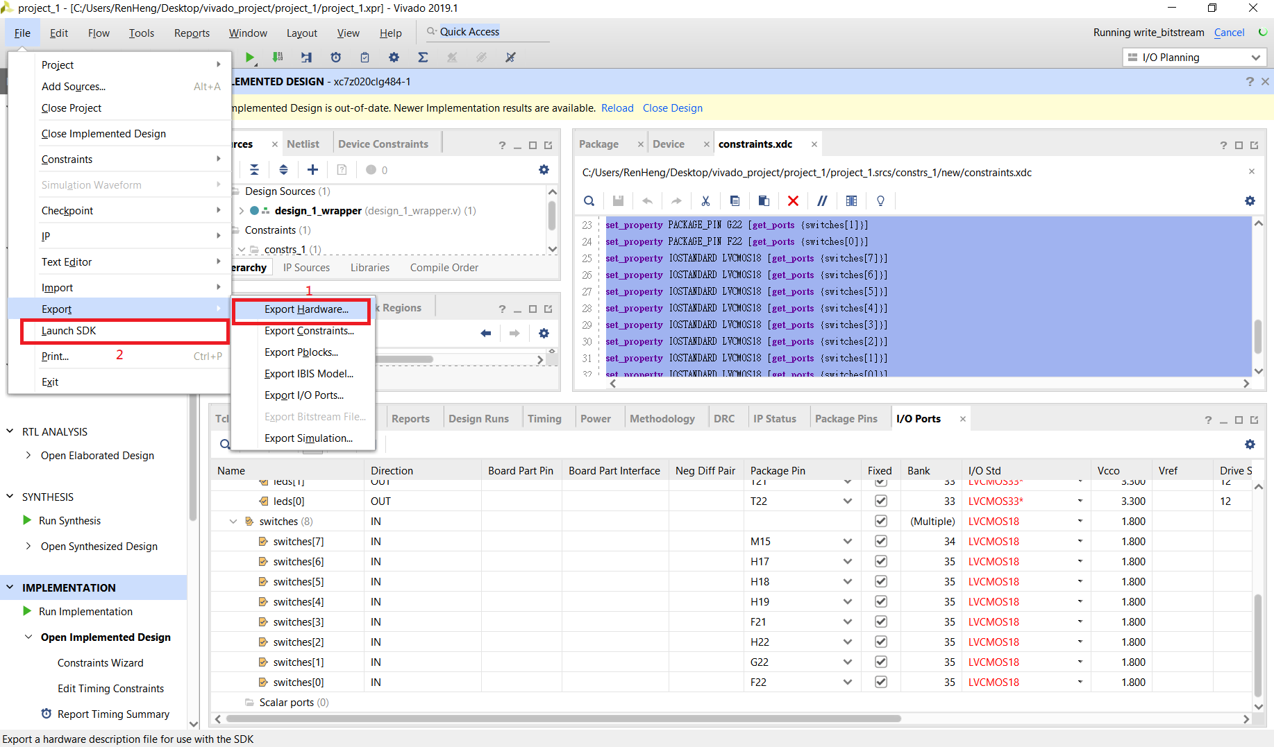
Run Synthesis -> Run Implementation -> Open Implementation Design -> Set Ports -> Ctrl + S -> constraints.xdc

1
2
3
4
5
6
7
8
9
10
11
12
13
14
15
16
17
18
19
20
21
22
23
24
25
26
27
28
29
30
31
32
set_property PACKAGE_PIN U14 [get_ports {leds[7]}]
set_property PACKAGE_PIN U19 [get_ports {leds[6]}]
set_property PACKAGE_PIN W22 [get_ports {leds[5]}]
set_property PACKAGE_PIN V22 [get_ports {leds[4]}]
set_property PACKAGE_PIN U21 [get_ports {leds[3]}]
set_property PACKAGE_PIN U22 [get_ports {leds[2]}]
set_property PACKAGE_PIN T21 [get_ports {leds[1]}]
set_property PACKAGE_PIN T22 [get_ports {leds[0]}]
set_property IOSTANDARD LVCMOS33 [get_ports {leds[7]}]
set_property IOSTANDARD LVCMOS33 [get_ports {leds[6]}]
set_property IOSTANDARD LVCMOS33 [get_ports {leds[5]}]
set_property IOSTANDARD LVCMOS33 [get_ports {leds[4]}]
set_property IOSTANDARD LVCMOS33 [get_ports {leds[3]}]
set_property IOSTANDARD LVCMOS33 [get_ports {leds[2]}]
set_property IOSTANDARD LVCMOS33 [get_ports {leds[1]}]
set_property IOSTANDARD LVCMOS33 [get_ports {leds[0]}]
set_property PACKAGE_PIN M15 [get_ports {switches[7]}]
set_property PACKAGE_PIN H17 [get_ports {switches[6]}]
set_property PACKAGE_PIN H18 [get_ports {switches[5]}]
set_property PACKAGE_PIN H19 [get_ports {switches[4]}]
set_property PACKAGE_PIN F21 [get_ports {switches[3]}]
set_property PACKAGE_PIN H22 [get_ports {switches[2]}]
set_property PACKAGE_PIN G22 [get_ports {switches[1]}]
set_property PACKAGE_PIN F22 [get_ports {switches[0]}]
set_property IOSTANDARD LVCMOS18 [get_ports {switches[7]}]
set_property IOSTANDARD LVCMOS18 [get_ports {switches[6]}]
set_property IOSTANDARD LVCMOS18 [get_ports {switches[5]}]
set_property IOSTANDARD LVCMOS18 [get_ports {switches[4]}]
set_property IOSTANDARD LVCMOS18 [get_ports {switches[3]}]
set_property IOSTANDARD LVCMOS18 [get_ports {switches[2]}]
set_property IOSTANDARD LVCMOS18 [get_ports {switches[1]}]
set_property IOSTANDARD LVCMOS18 [get_ports {switches[0]}]

Run Implementation -> Generate Bitstream -> Open Hardware Manager -> Auto Connect -> Program
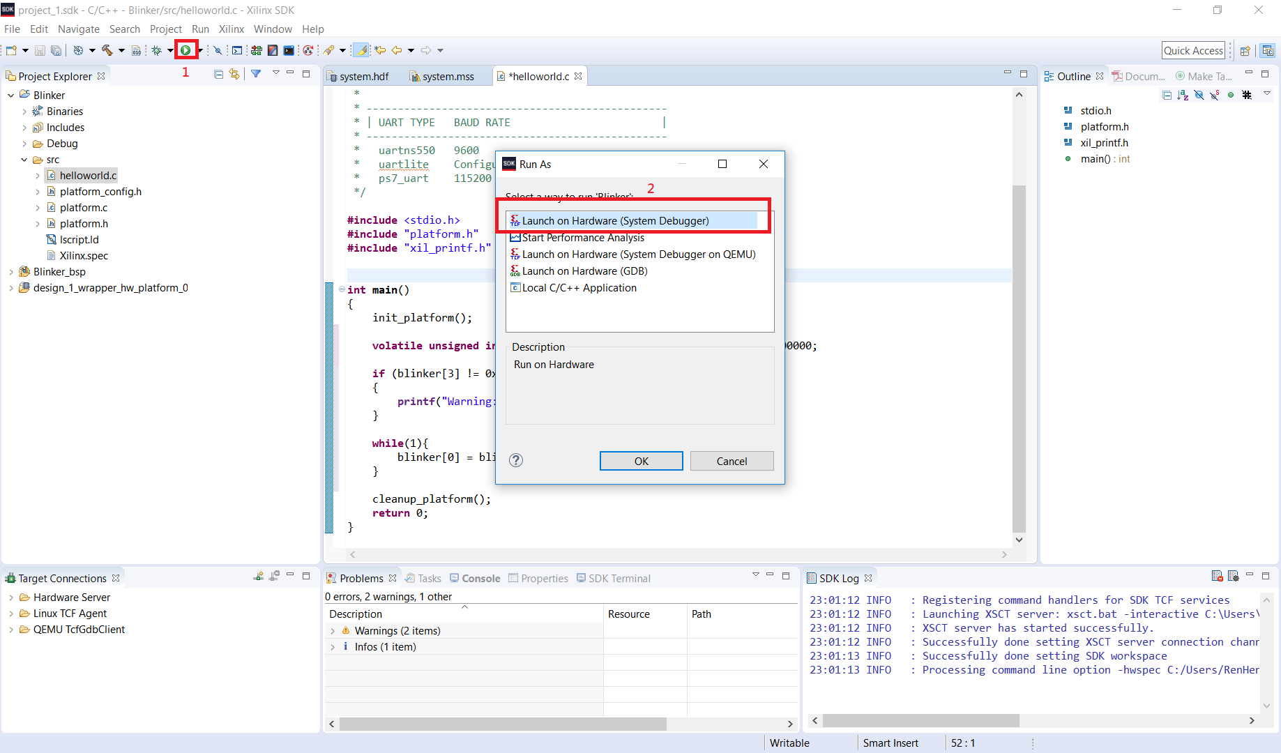
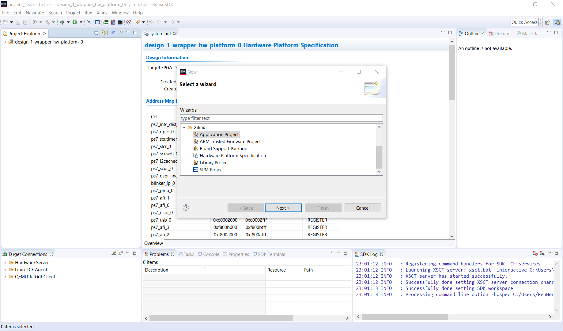

3、Launch SDK

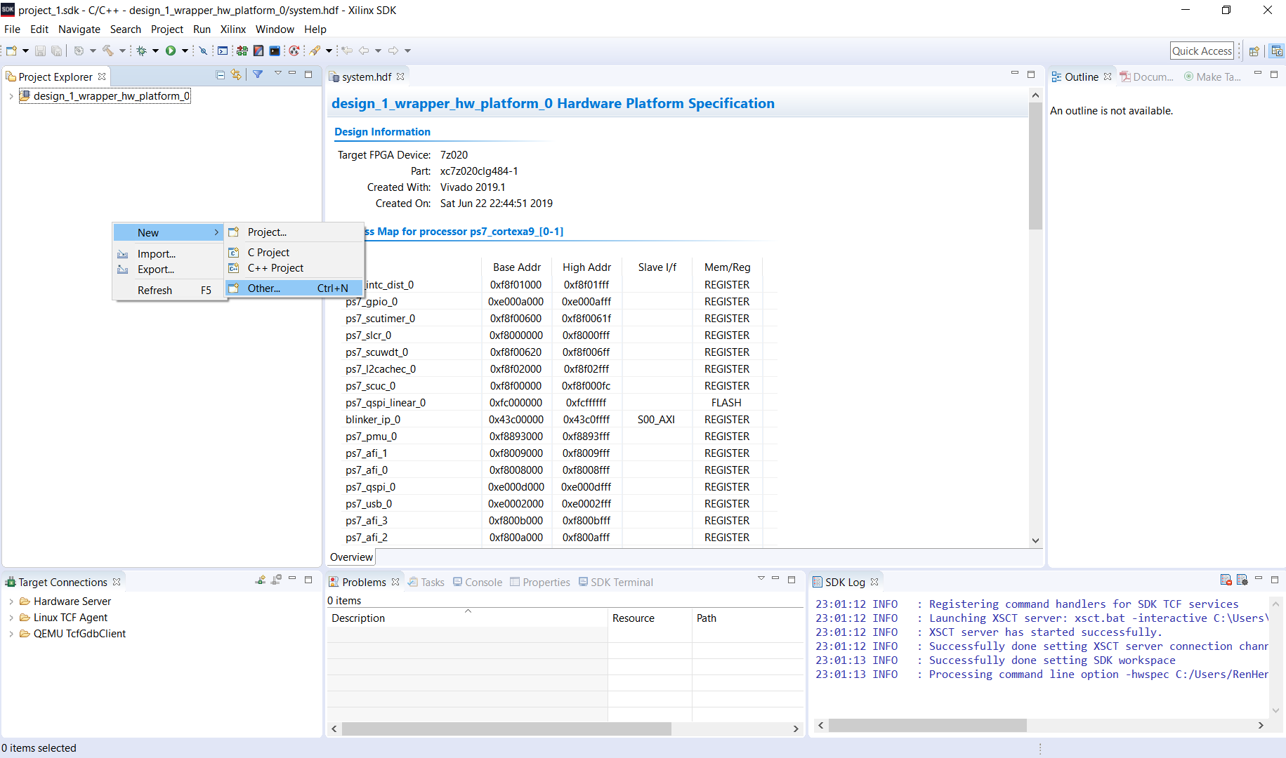
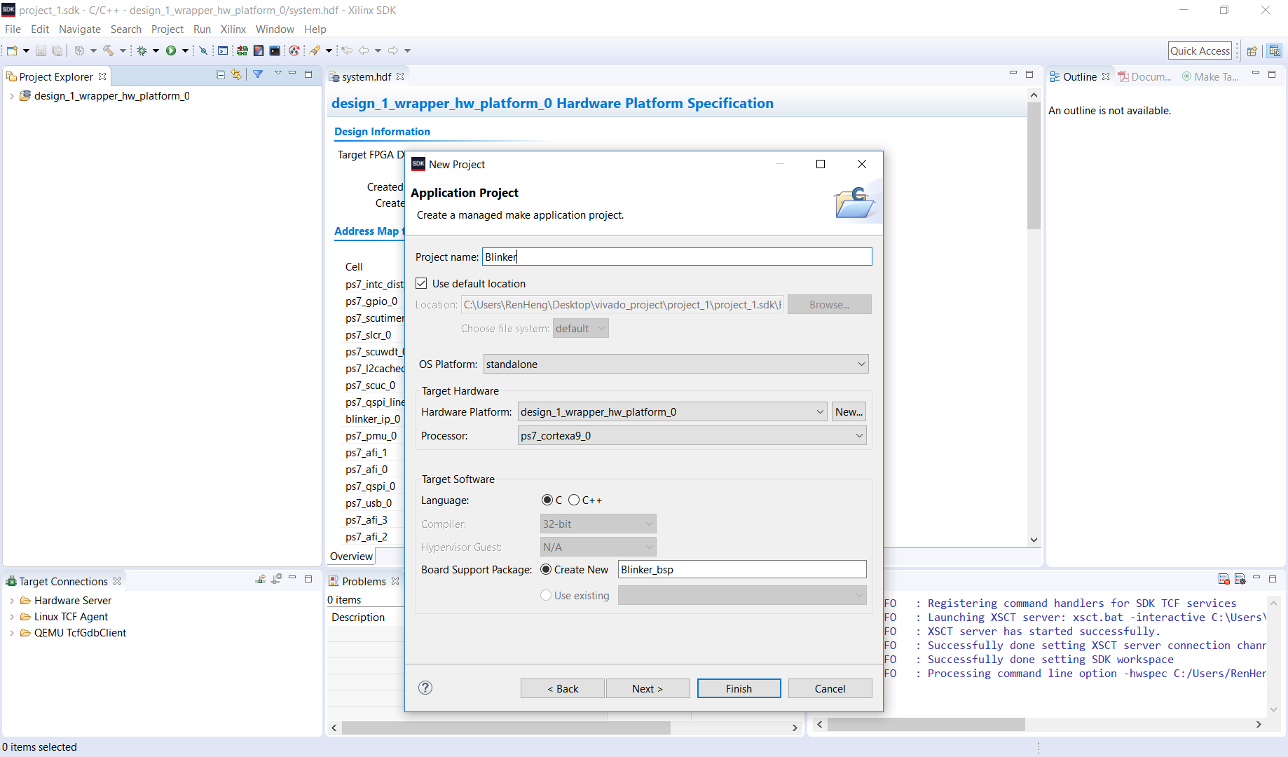
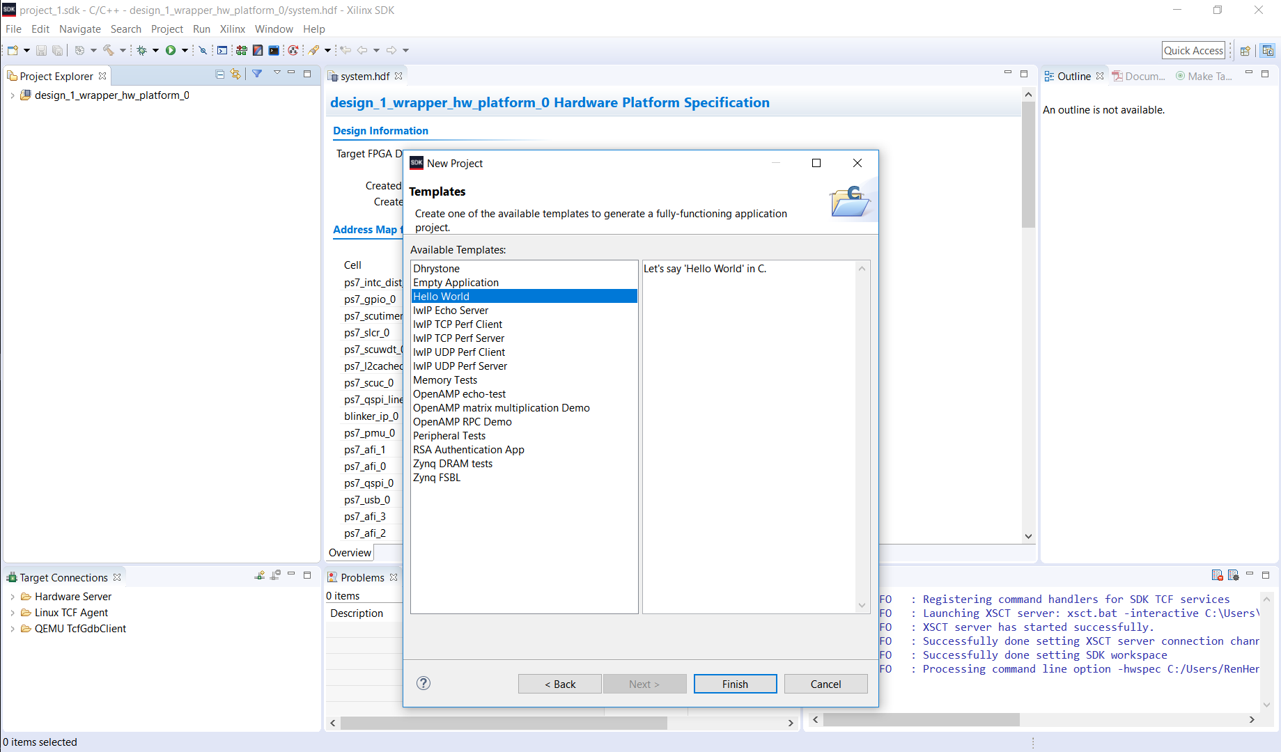
Project Export hardward (check include bitstream) -> launch SDK -> New C project
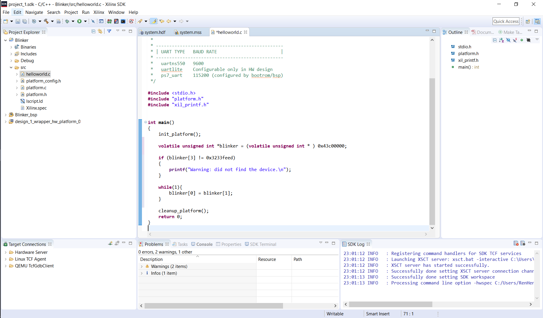
1
2
3
4
5
6
7
8
9
10
11
12
13
14
15
16
17
18
int main()
{
init_platform();

volatile unsigned int *blinker = (volatile unsigned int * ) 0x43c00000;

if (blinker[3] != 0x3233feed)
{
printf("Warning: did not find the device.\n");
}

while(1){
blinker[0] = blinker[1];
}

cleanup_platform();
return 0;
}

Now your leds will be turned on by switches.


Reference

Vivado Custom IP with Memory Mapped I/O

Basic FPGA Tutorial